B.Tech in Semiconductor Engineering
January 30, 2026 2026-03-21 12:31B.Tech in Semiconductor Engineering
Welcome to B.Tech in Semiconductor Engineering
Welcome to B.Tech in Semiconductor Engineering
Director’s Desk
Dr. Sanjeev Sharma
Director- School of Mechatronics Engineering
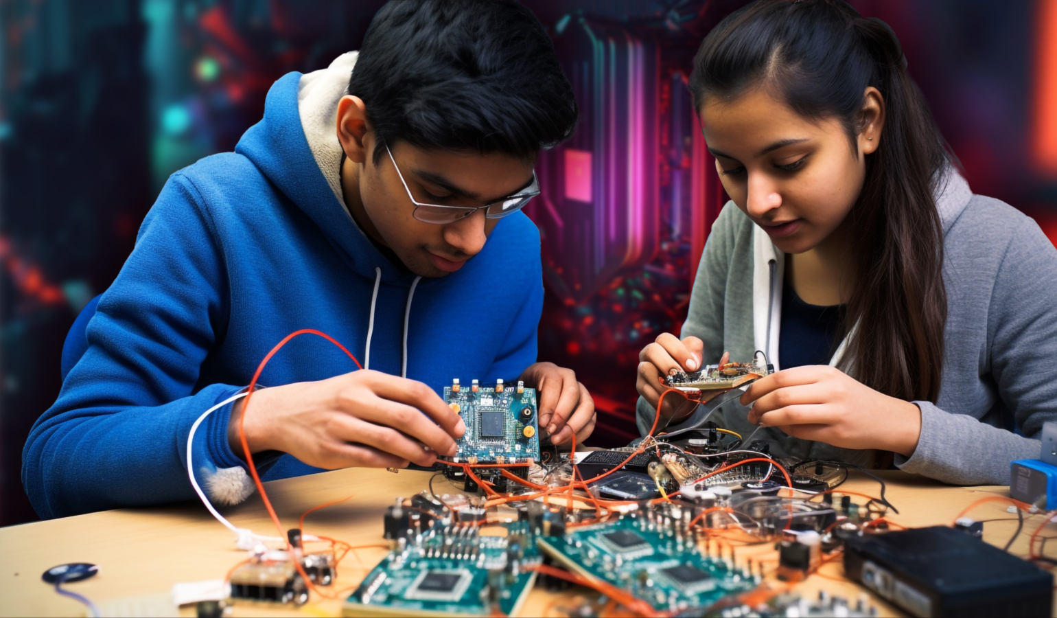
Semiconductors are the invisible engines powering the modern world. From Artificial Intelligence, electric mobility, and smart manufacturing to defence systems, space technologies, and next-generation communication, semiconductors form the backbone of every advanced technological ecosystem. As India moves into a decisive decade of technological self-reliance, semiconductor capability will play a defining role in shaping economic growth, national security, and global competitiveness.
At Symbiosis Skills & Professional University (SSPU), the B. Tech in Semiconductor Engineering has been conceptualized with a clear and focused vision: to create industry-ready engineers equipped with strong fundamentals, hands-on skills, and global exposure in semiconductor design and VLSI technologies. The programme has been carefully benchmarked against leading national and international institutions ensuring academic rigor, relevance, and future readiness.
Strategically located in Pune, one of India’s fastest-growing hubs for semiconductor design centers and Global Capability Centers (GCCs), SSPU offers students a distinct advantage through close industry interaction, internships, live projects, and exposure to real-world semiconductor workflows. We invite aspiring engineers to be part of India’s semiconductor journey and contribute to building technologies that will define the future.
At Symbiosis Skills & Professional University, this programme has been designed with a clear vision: to create industry-ready semiconductor engineers who can design, innovate, and lead in a global technology ecosystem. Benchmarking leading institutions such as IITs, IISc, NITs, and top private universities, this programme blends strong academic fundamentals with deep industry integration.
Located in Pune – one of India’s fastest-growing semiconductor and GCC hubs, the programme offers students a unique advantage through industry exposure, hands-on learning, and career-focused training. We invite aspiring engineers to be part of India’s semiconductor journey and shape the future of technology.
Why B. Tech. Semiconductor Engineering?
- India’s semiconductor market projected to exceed USD 100 Billion by 2030
- 1 Million+ jobs expected in the next five years
- 3 lakh skilled engineer gap by 2027
- Strong Government of India support through India Semiconductor Mission & PLI Schemes
- High-growth careers with 15–20% CAGR across design, testing, and packaging
This programme prepares students not just for jobs but for long-term, future-proof careers.
Eligibility Criteria
Eligibility Criteria
- Passed 10+2 (HSC or equivalent) from a recognized board
- Physics and Mathematics as compulsory subjects
- Chemistry / Biotechnology / Biology / Technical Vocational subject as one of the optional subjects
Programme Structure
Duration: 4 Years (8 Semesters)
Programme Highlights
- Strong ECE foundation with focused semiconductor specialization
- Progressive learning from fundamentals to advanced VLSI design
- Industry-driven curriculum aligned with global benchmarks
- Mandatory industry internships and live projects
Curriculum Snapshot
- Semiconductor Physics & Materials
- Analog and Digital VLSI Design
- CMOS Technology & Device Fabrication Basics
- Physical Design & Verification
- Semiconductor Testing & Advanced Packaging (ATMP)
- EDA Tools Training (Cadence, Synopsys – industry-standard flows)
- Capstone Project with industry or research focus
Industry Exposure & Learning Ecosystem
- MOUs with leading semiconductor companies and GCCs
- Internship pipelines with Cadence, NXP, Marvell, Lattice, Alphawave and ecosystem partners
- Guest lectures, masterclasses, and workshops by industry experts
- Access to EDA tools, simulation labs, and project-based learning
- Opportunities for joint research, innovation, and startups
Fee Details For Indian Student
| (New Admission – 2026-27) | ||||
| Caution Money | Academic Fees | Total Fees | 1st Installments | 2nd Installments |
| At the time of Admission | Due Date – 31-10-2026 | |||
| 10,000 | 2,94,500 | 3,04,500 | 1,64,500 | 1,40,000 |
| Hostel Charges | ||
| 1 | 2 Seater Non-AC Rooms | 2,05,000 |
| 2 | Hostel Caution Money (Refundable) | 15,000 |
Fee Deatils For NRI Student
| (New Admission – 2026-27) | ||||
| Caution Money | Academic Fees | Total Fees | 1st Installments | 2nd Installments |
| At the time of Admission | Due Date – 31-10-2026 | |||
| 10,000 | 3,49,500 | 3,59,500 | 1,92,000 | 1,67,500 |
| (Existing Students-2026-27) | ||||
| Academic Fees | 1st Installments | 2nd Installments | ||
| Due Date – 31-07-2026 | Due Date – 31-10-2026 | |||
| 3,49,500 | 1,82,000 | 1,67,500 | ||
| Hostel Charges | ||
| 1 | 2 Seater Non-AC Rooms | 2,05,000 |
| 2 | Hostel Caution Money (Refundable) | 15,000 |
Career Opportunities
Graduates of this program are prepared for high-demand roles such as:
- VLSI Design Engineer
- Physical Design / Verification Engineer
- Semiconductor Process Engineer
- Test & Validation Engineer
- Advanced Packaging & ATMP Specialist
- EDA Application / Support Engineer
- Research & Development Engineer
Career Pathways
- Global semiconductor companies & GCCs
- Fabless design houses and startups
- OSAT / ATMP companies
- Research labs and higher studies (M.Tech / MS / PhD)
- Entrepreneurship in semiconductor design and deep-tech startups
Program Highlights
- Industry-aligned postgraduate programme blending energy engineering fundamentals with sustainability thinking and applied skills
- Curriculum benchmarked against leading national/international institutions while contextualised for industry deployment
- Strong focus on hands-on laboratories, live projects, internships, and consultancy assignments
- Designed within SSPU’s Skill University framework, emphasising employability, entrepreneurship, and applied research
- Alignment with NEP-2020, enabling flexibility, experiential credits, and industry participation
- Exposure to green jobs, emerging energy technologies, and climate-resilient energy systems
Why Choose SSPU for M.Tech (Energy Engineering)?
With its unmatched skill-based university model, national recognition, industry integration, and sustainability-first vision, SSPU offers a programme that does not merely award a degree—but builds future-ready energy leaders grounded in ethics, employability, and real-world impact.